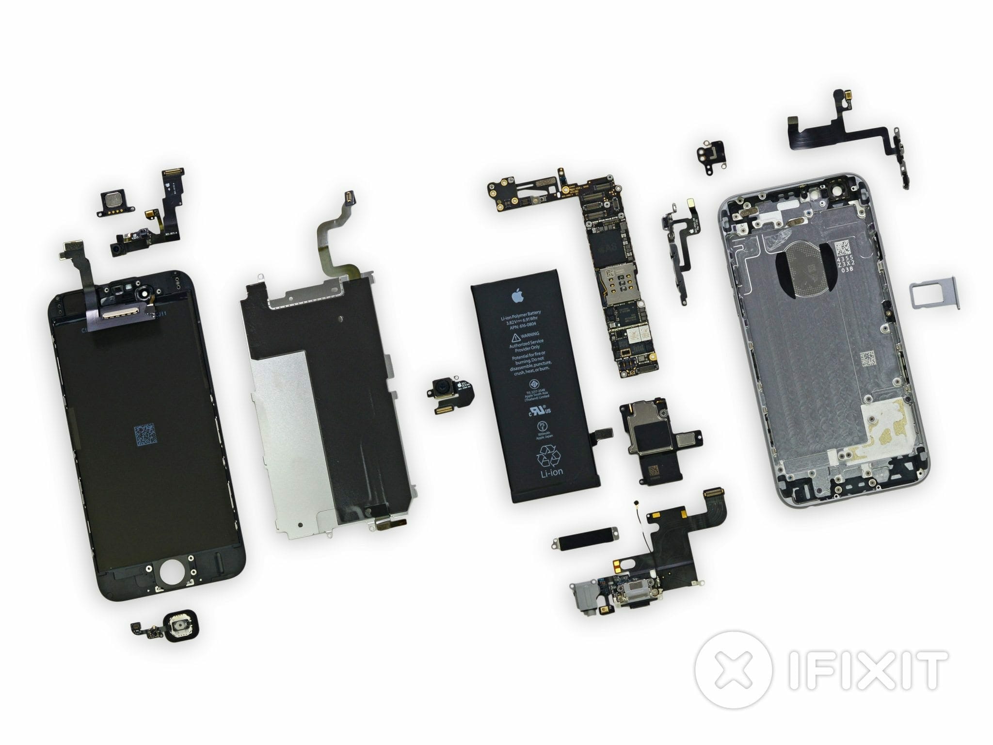
This has now been the waiting moment for all of us. The Apple iPhone 6 teardown is now brought to you by the guys at iFixit. As per usual, it is done very professionally and the phone has been rated 7/10 for repair ability, just like its elder brother.
After the iPhone 6 teardown was complete, the gurus at iFixit did not like the proprietary pentalobe screws used by Apple and express their objection of Apple not sharing repair information with independent repair shops.
Well there is an upside to the iPhone 6 teardown that the 1810 mAh battery removal process is straightforward and the display assembly comes out of the phone first, it makes repairing a damaged screen easier than it used to with previous models. To finish off, the fingerprint sensor cable has been rerouted and thus making the phone more safe than the iPhone 5s.
Now here we reach to the more technical side of iPhone 6 teardown, the teardown showcases the main logic board of the iPhone 6. It consists of the Apple A8 system-on-a-chip, which neighbors the SK Hynix 1GB RAM. Then there is the 16GB NAND flash chip made by Sandisk. Which depends on the storage capacity of your iPhone.
The teardown also discloses some tidbits such as the new and, presumably, improved vibrator assembly. It is with a linear oscillating design compared to the iPhone 5/5s counterweight design.
Now here is the slideshow of the iPhone 6 teardown.

